PNP 6600 EVOf Flip Chip Die Bonder

The PNP6600 multifunctional high-precision die bonding machine is mainly used in the semiconductor packaging industry and can be used for various types of integrated packaging.
Product
Center
Home / Product center / PNP 6600 EVOf Flip Chip Die Bonder

flip chip
Automatic 180 ° Flip

Ultrasonic bonding system
Alignment accuracy 0.1 μ m

Non contact height measurement,
Accuracy ± 5 μ m, can measure one stick one

Automatic compensation system
It can automatically compensate according to the actual production and installation situation, ensuring the installation accuracy of the equipment during the production process

Self checking device function module
One click start of device basic performance testing, reducing the threshold for use and ensuring device accuracy

Automatic calibration after installation:
Automatically calibrate according to set conditions

PROCESS
 
Specifications
Accuracy
  • X/Y mounting accuracy (calibration sheet)

    ±5um@3σ

  • θ placement accuracy (calibration piece)

    ±0.1@3σ

  • Power control range

    50g-5kg(Optional 10g-1kg)

  • Power control accuracy

    10-200g±5g >200g-1kg±10g >1kg±5%

CPH
  • reflectance standards

    CPH2500(±10um@3s )/CPH2000(±7um@3s )/CPH1500(±5um@3s)
  • Inverted process

    When the process time is 50ms, it is the same as the standard CPH, but the actual efficiency is affected by the customer's process time

Bond Heads
  • standard

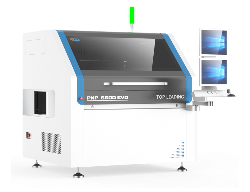
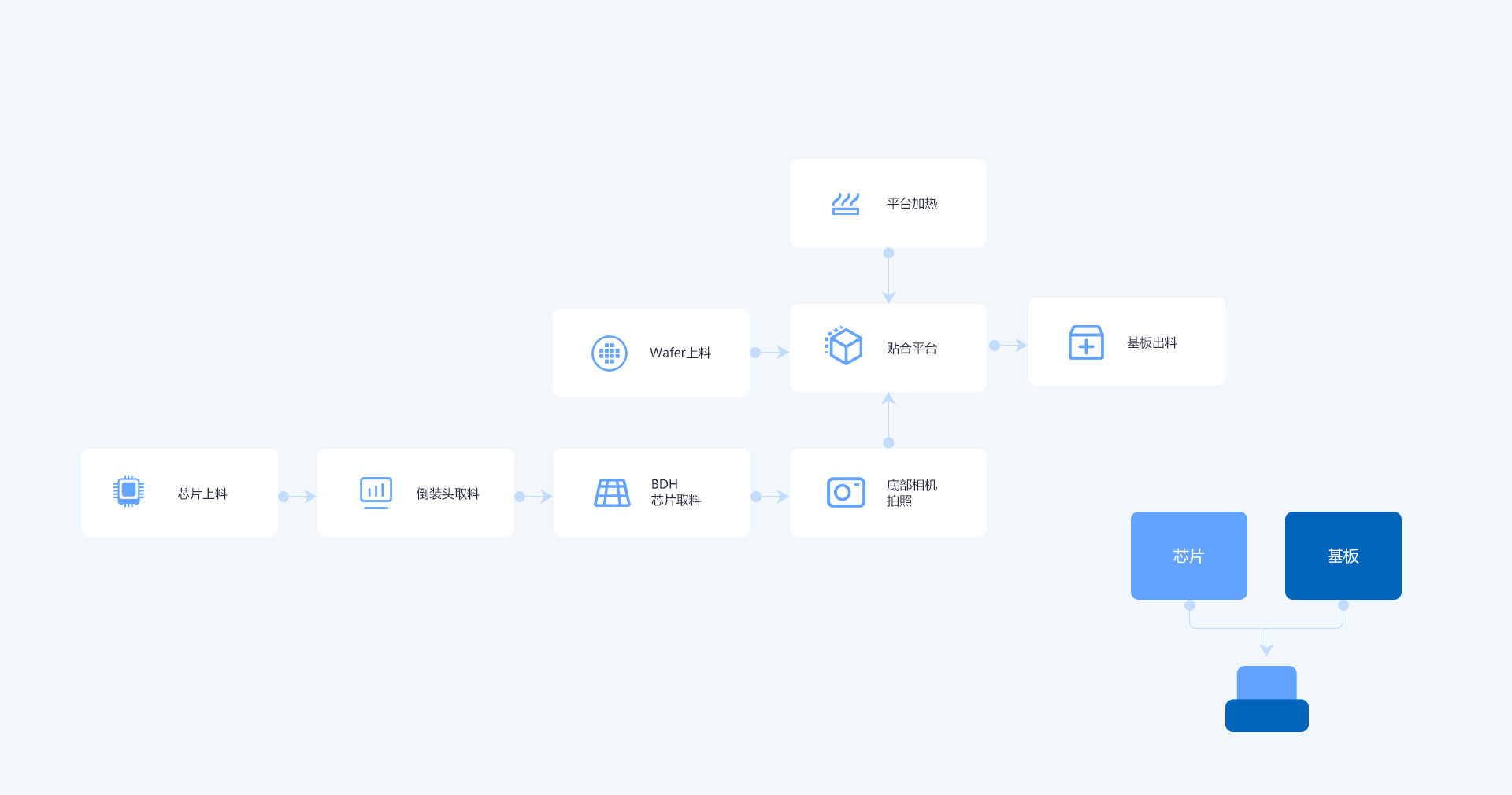
    Single mount head+inverted head

  • rotate

    0°- 360°rotate


Machine size

  • Length * Width * Height

    1650mm x 1600mm x 1800mm


Wafer
  • Chip Size

    0.5-70mm

  • chip thickness

    >50μm

  • Wafer size

    4-12 inches (compatible with 3 * 6 inch mother and child rings)

  • frame size

    FF070,FF105,FF108,FF123;modifiable
Tray Disk
  • Waffle pack/Gel-Pak

    2*2英寸5個(gè)(可選14/35個(gè)),4*4英寸(4個(gè))

  • Other requirements

    Jedec trays, etc


Substrate and carrier
  • type

    FR4,ceramic,BGA, flex,boat,lead frame,waffle pack
    Gel-Pak®,JEDEC tray, odd-shape substrates

  • Platform heating

    MAX350 ° C with inert gas atmosphere protection

  • Scope of substrate work

    300mm x 200mm


statistics
  • uptime

    >98%

  • Yield

    >99.95%


optional
  • hardware

    Open platform architecture for complete customization

  • software

    Single component tracking, CAD download, wafer mapping, substrate mapping, barcode scanner, data matrix recognition, etc


Data Request

hello!

Data Request

Hotline

(86)020-84657805
Data Request

Apply now

* This information is only used to contact you and help you better understand our information and products.