Please enter your search product keyword


Multiple material thin film circuits, thick film circuits DPC、 Microstrip filters, thin film attenuators, power heat sinks, etc
Whole ceramic substrate, blue film, expansion ring
Automatic correction of feeding angle
Maximum support0*320mm
Support importing multiple layers of DXF/DWG/GBR drawings
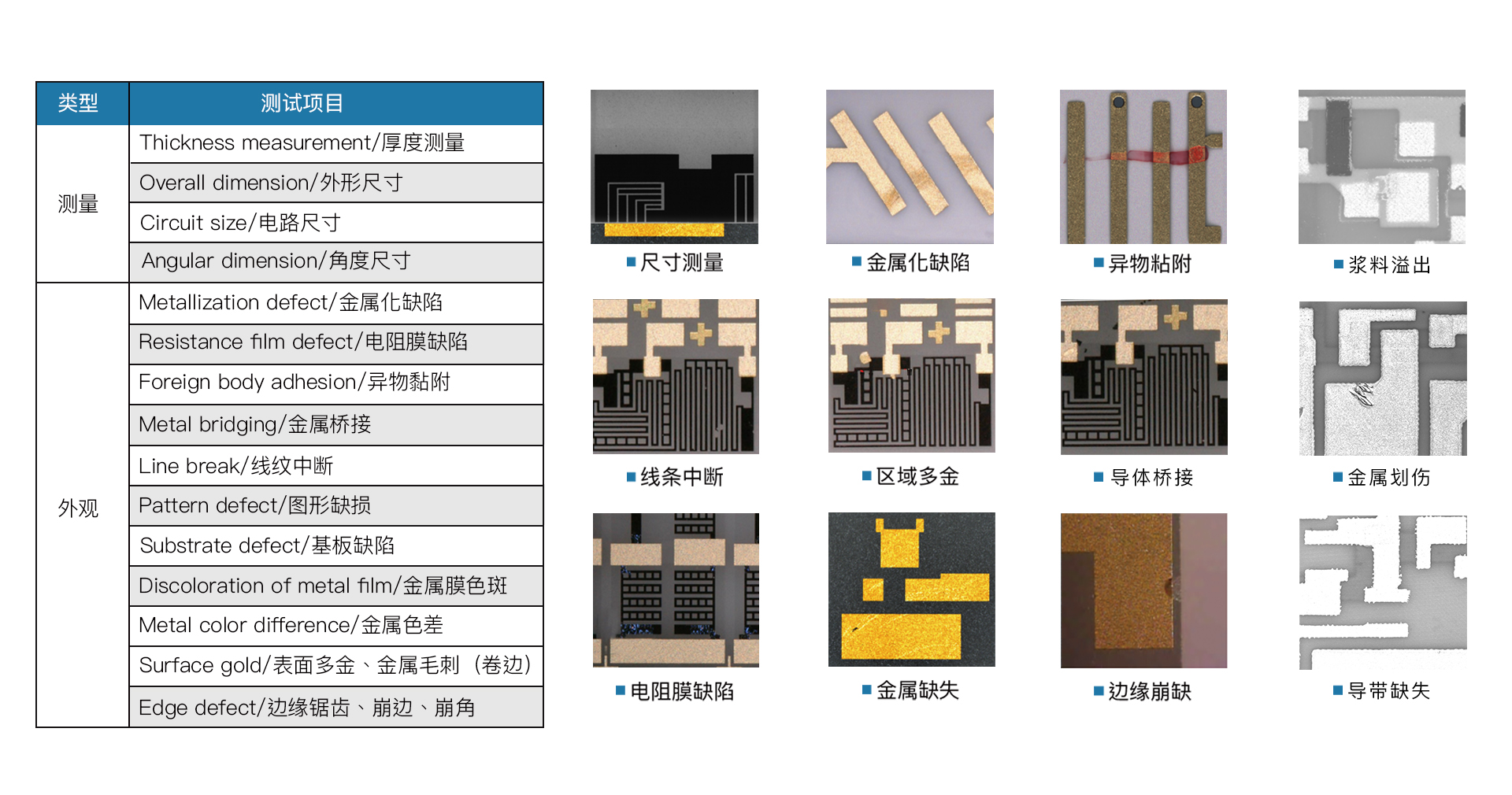
Measurement of external dimensions, 3D thickness measurement, circuit size measurement, planar defect detection, stereoscopic defect detection
Can be equipped with cameras ranging from 5 million pixels to 65 million pixels, selected according to detection needs
Minimum repeatability accuracy ± 1um (may vary depending on the selected camera accuracy)
Minimum recognizable accuracy ≥ 5um (may vary depending on the selected camera accuracy)
Minimum repeatability accuracy ± 50nm
Minimum recognizable accuracy ≥ 10um (may vary depending on the selected camera accuracy)
Multi layer algorithm independently sets tolerance+visual AI deep learning defect classification
Inkjet marking or laser marking or graphic report
Real time monitoring, data storage, and data statistics functions for detection data
60s-120s/slice(The final efficiency will depend on the type of defect detected, the number of defects, and the size of the product)
It can be equipped with batch/work order/product scanning and character OCR recognition functions, and can add silo components+motion modules or robotic arms to achieve fully automatic loading and unloading. It can also be equipped with offline software analysis function to perform overall statistical analysis on stacked data